Thin film materials are an important part of modern materials science. The laboratory deals with fundamental synthetic issues and with scientific basis of thin film production technology:
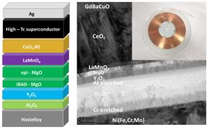
– High-temperature superconductors and buffer layers
– Materials with colossal magnetoresistance
– Ferroelectric materials
– Multiferroic materials
– Metal-insulator transition materials
– Transparent conductors
– Upconversion materials
For chemical synthesis of thin film materials we use MOCVD and MOCSD techniques.
Metal Organic Chemical Vapor Deposition (MOCVD)
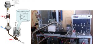
This method is based on transfer of volatile metal compounds – precursors – at relatively low temperatures (200-300°С) in inert atmosphere to the reactor where they undergo oxidation/hydrolysis/ thermolysis which results in formation of thin film of inorganic materials on the substrate.
MOCVD technique allows obtaining thin film materials on single crystalline and metal ribbon substrates. Each material requires thorough optimisation of synthetic conditions and composition of precursor mixture. This is why we use our original in-house MOCVD apparati and are always in development of the new hardware and new metal-organic precursors.
Metal Organic Chemical Solution Deposition (MOCSD)
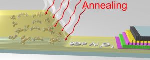
MOCSD uses the solutions of metal carboxylates as precursors. Film deposition is performed by dip-coating technique. The good precursor solution which wets the substrate, gives the uniform gel film after solvent removal, and completely decomposes at high temperatures resulting in desired compound is a key to this technique.
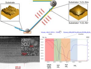
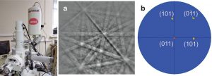
For analysis of thin film materials in terms of their composition, morphology and texture we use SEM, TEM, AFM, EBSD, EDX methods, and various XRD techniques including θ-θ scan, φ scan, ω scan, pole figures, in-plane 2θχ-φ scan, grazing incident 2θ scan.